Developer Tools●●●Banger
Tapflow – self-hosted iOS/Android simulator streaming for mobile QA
Self-hosted simulator streaming beats BrowserStack on privacy and recurring costs.
Solve My ProblemBig Brain
duchanjo
401mo ago
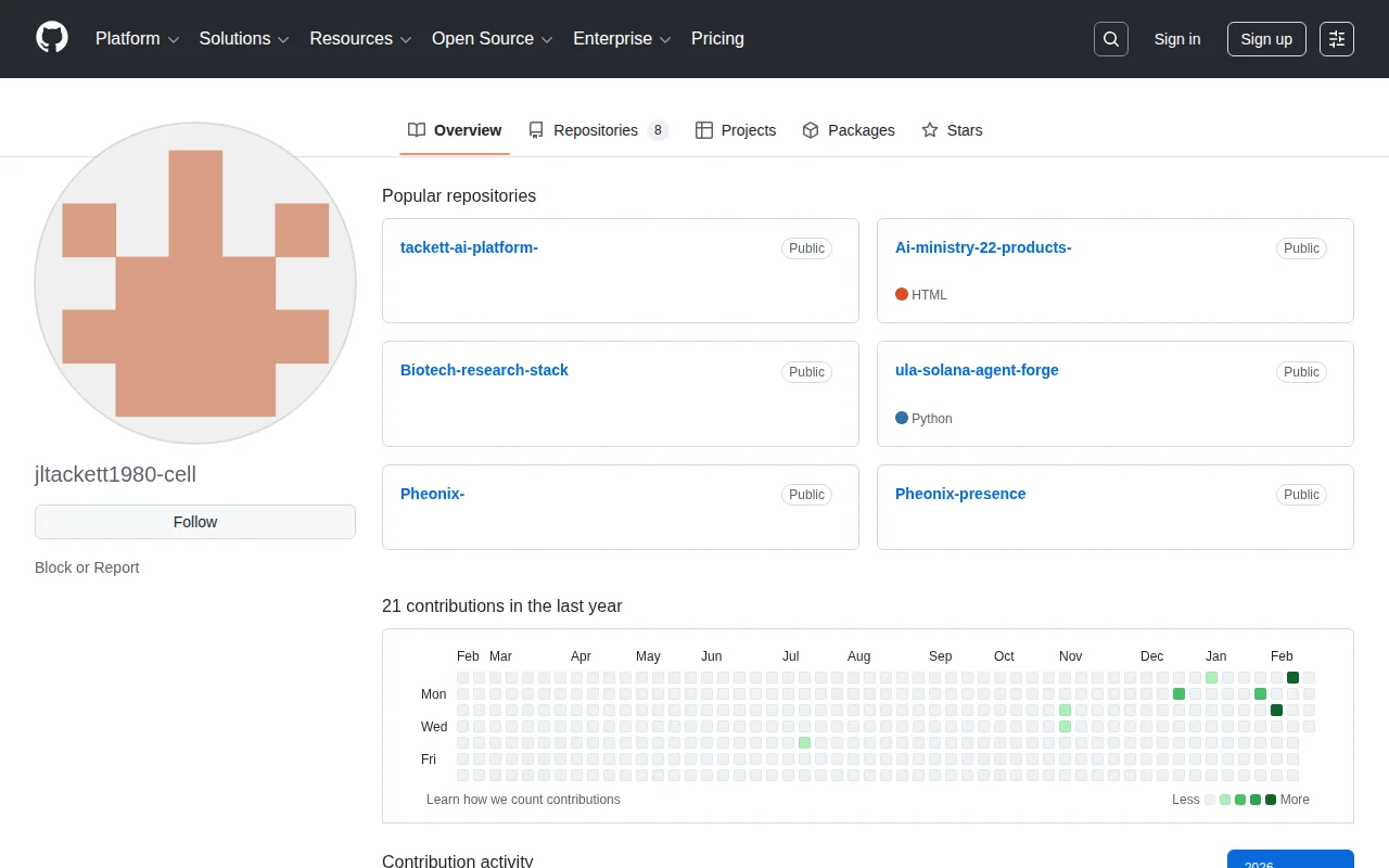
Simulating a 16,777,216-MAC analog in-memory Phoenix SoC on a $60 Android using iverilog and Yosys is an audacious technical flex — the repo claims end-to-end verification (adders → ALUs → RISC‑V core → FPU) and a working 8-bit CPU. It's simulation-only and the writeup could do more to make reproduction trivial, but the ULA plain-English compiler and the no-cloud, mobile-only build story make this a rare outsider contribution to EDA.
Chip designers, semiconductor / EDA engineers, RISC‑V and hardware hackers, systems architects interested in in-memory compute
Phoenix 4096×4096 specs: - 16,777,216 MAC units (analog in-memory compute) - 50,331 TOPS @ 3GHz (25× NVIDIA H100) - 512 deterministic reasoning cores - 2 TB/s memory bandwidth - All verified in simulation
Hardware verified (15/15 passing): - Half Adder → Full Adder → 8/16/64/128/256-bit ALUs - 8-bit CPU (Fibonacci working) - RISC-V core - FPU (IEEE 754) - GPU SIMD - Complete Phoenix SoC
Also built: - ULA compiler: Plain English → 12 languages (Python, Rust, Java, Assembly, COBOL, Fortran, C, C++, Go, Kotlin, Solidity, TypeScript) - RF presence detection: 2-person tracking via WiFi signals, no cameras, 91% gesture accuracy
All code on GitHub: https://github.com/jltackett1980-cell
Built in Sikeston, MO on a $60 Android. No laptop. No cloud. No funding.
Looking for: Chip designers, semiconductor engineers, anyone interested in open silicon or analog computing. Want to tape out with Efabless or similar.
Live demo available
Self-hosted simulator streaming beats BrowserStack on privacy and recurring costs.
Fingerprints hardware interaction graphs to catch trojans functional testing misses.
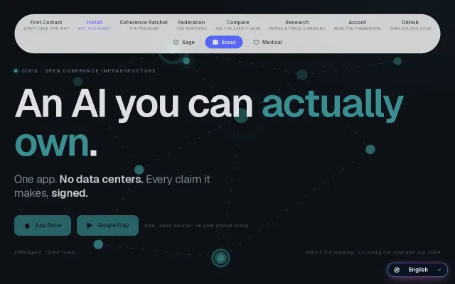
Signed AI claims you can verify and undo—unlike black-box cloud models.
Piping accelerometer data through audio filters to flash keyboard lights is genuinely wild.
Turns a friend's Android into a geo-spoofing exit node without paying for a VPN.
TPM-anchored agent identity solves a real problem, but product is vaporware—coming soon, no code yet.